Thank you for the kind words.
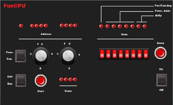
Here is the front panel as it was originally planned:
Here one can see the modules scattered all around of version 1.
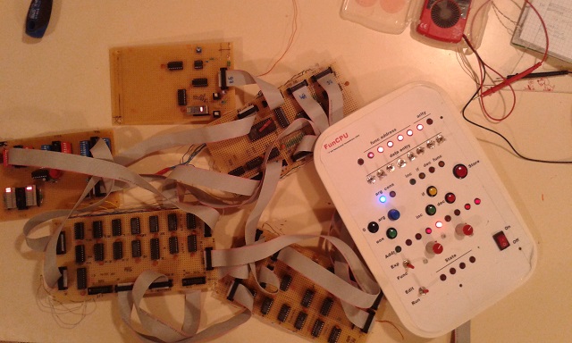
It was my first attempt, and resulted in a rather chaotic design and implementation. It is needless to say that it was not working. It almost worked, but not quite.
I created a new version. Version 2 had to be rebuilt it from scratch, using a little more reliable and disciplined approach. Here is the register module of the second build:
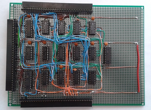
It is constructed from four modules plus the control board, using 74HC components and 4 EPROMs (3 used for micro-sequencer and one for the tokenizer for the tagged architecture) and one 32K SRAM.
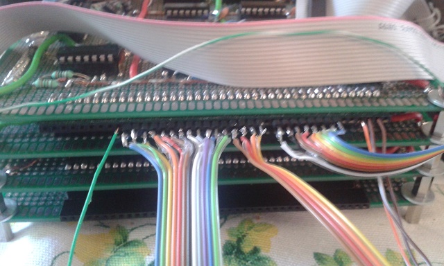
The modules are stacked one on another. They are interconnected via 3 buses each with 40 pins.
Here one can see the stacked boards. Please notice that testing can be done just by looking at the 120 exposed pins. These pins more or less describe the full behaviour of the CPU at any moment in time.
Approximately 30 ICs were used for the CPU itself, and another 15 ICs were required to implement the interface. (These 45 components include the ROMs and RAM as well). This is needed to communicate with the CPU, i.e. to enter and read data.